India's first front-end 300mm commercial semiconductor fabrication facility.
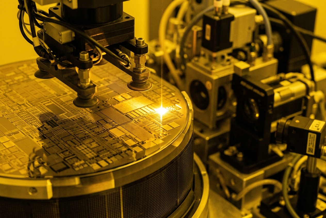
Tata Electronics is building India's first front-end 300mm commercial semiconductor fabrication plant at Dholera SIR in partnership with PSMC Taiwan. The total investment stands at $11 billion (approximately ₹91,000 crore), making it the single largest industrial investment in Gujarat's history. At full capacity, the facility will produce 50,000 wafers per month. The target product line covers mature nodes in the 28 to 110 nanometer range, used for power management ICs, display drivers, microcontrollers, and HPC logic chips.
The global conversation around semiconductors tends to focus on cutting-edge chips, the 3nm and 5nm processes used in smartphones and AI accelerators. But mature nodes tell a different story. Every electric vehicle on the road needs dozens of power management chips. Every display panel requires driver ICs. Industrial automation, IoT sensors, and medical devices all rely on chips fabricated at 28nm and above. This segment of the market generates roughly $40 billion annually in pure-play foundry revenue, rising to about $60 billion when including integrated device manufacturers. Tata's fab is targeting that steady, high-volume demand rather than competing at the bleeding edge. It is also a strategic stepping stone: mastering mature-node process control builds the engineering base needed for future advancement.
The public subsidy for this project is substantial. The central government contributes a 50% capital subsidy through the India Semiconductor Mission. The Gujarat state government adds another 20%, plus subsidized land, reduced power tariffs, and stamp duty concessions. Together, that means roughly 70% of the project cost is covered by public funds. The remaining 30% comes from Tata Electronics and its partners. A consortium loan of ₹168.35 billion (about $735 million) has been secured from HSBC, MUFG, First Abu Dhabi Bank, DBS, and ANZ, routed through GIFT City. Tata Group must retain a minimum 51% majority stake in the special purpose vehicle (TSML) and maintain a specified debt-to-equity ratio through 2031.
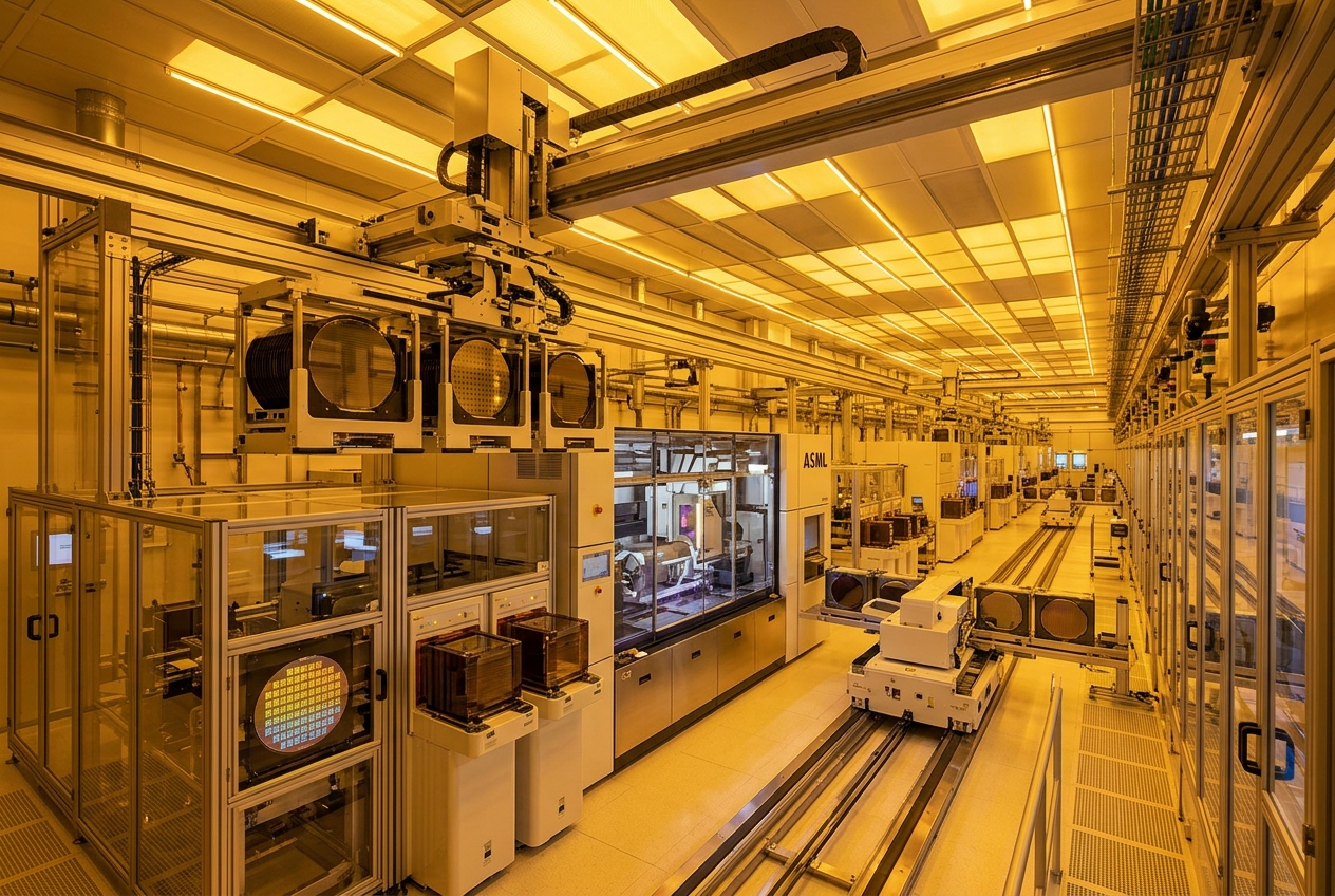
ASML is providing the DUV lithography equipment, the most critical and expensive tool in any fab, with a memorandum of understanding signed in May 2026. Tokyo Electron supplies process equipment. Synopsys handles the electronic design automation software. The commercial off-take agreements anchor demand: Analog Devices, Himax, and Bharat Electronics Limited (BEL) have all signed agreements to purchase chips from the facility. Intel signed a collaboration agreement in late 2025 covering manufacturing and packaging. The facility occupies a 66.166 hectare plot within the Dholera SIR Special Economic Zone. The entire operation is designed as an Industry 4.0 "lights-out" manufacturing environment, meaning it runs fully automated with minimal human intervention on the production floor.
A semiconductor fab of this scale does not operate in isolation. It requires a surrounding supply chain of equipment suppliers, specialty chemical vendors, gas suppliers, wafer polishing firms, packaging houses, and testing facilities. Each of these needs to locate within reasonable distance to serve the fab efficiently. That is how semiconductor clusters form, from Hsinchu in Taiwan to Portland in Oregon. Dholera's planners built the infrastructure to attract exactly these firms: plug-and-play industrial plots, reliable power from the solar park, zero-liquid-discharge water treatment, and direct access to Mundra Port for importing specialty materials. The Tata fab acts as the anchor tenant, and the supply chain fills in around it.
Semiconductor manufacturing demands a specific workforce profile. The fab will need process engineers, equipment technicians, cleanroom operators, quality control specialists, and chemical engineers, among others. At full capacity, employment runs into thousands of direct positions, with additional jobs in support services and the supply chain. This is where the education district becomes critical. The Gujarat Special Education Region is building programs specifically aligned to semiconductor skills: materials science, nanotechnology, electrical engineering, and advanced manufacturing. The timeline is deliberate. Academic operations begin in 2027, and the fab ramps production over the same period. The pipeline of trained graduates arrives as the fab scales up.
The fab depends on the solar park for clean power, the data centers for computational loads, and the expressway and port for logistics. Each piece of the Dholera ecosystem reinforces the others. But the fab also does something less visible: it signals to global investors that Dholera can execute complex, capital-intensive projects. When Tata chooses a location for an $11 billion facility, other companies take notice. The supply chain firms, the equipment vendors, the service providers, they all factor that decision into their own site selection. The fab is not just a factory. It is a proof point for the entire Dholera proposition.
← Back to Industries